 Lauri Pirttiaho
Electronics
Microcontroller
Once upon a time the Cypress PSoC4 prototyping kit was one of the cheapest ARM microcontroller boards available. With a resourceful microcontoller and an USB-serial adapter it has been one of my favorites for quick prototyping.
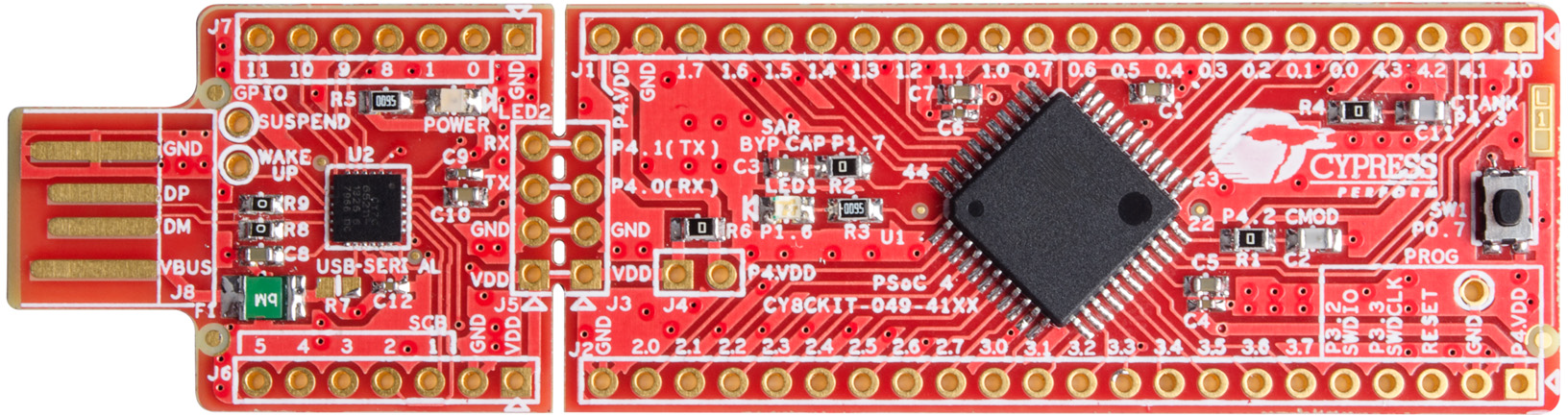
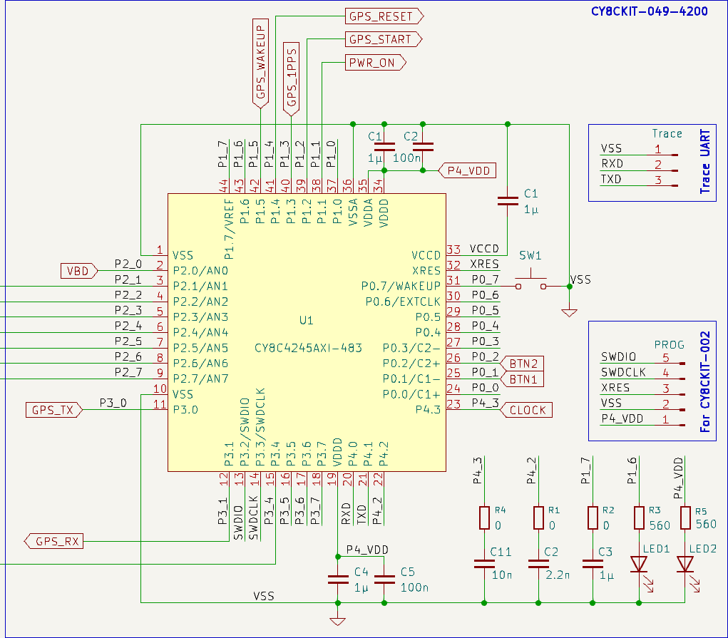
By now the kit is obsolete unobtainium but because of the cheap price I'd guess also many fellow hackers collected a lifetime stockpile of these. The kits I have been using are the 42xx variants with CY8C4245AXI-483 on board: Cortex-M0 at 48 MHz, 32 kB FLASH, 4 kB RAM.
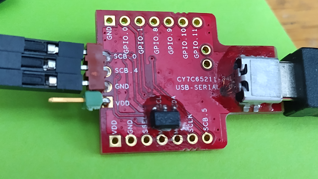
After completing a project and burying the µC board into a device the USB to serial adapters that were broken off from the kit have found other assignments as standalone adapters, usually with USB mini B socket glued on the USB finger to allow a cable between the adapter and PC.
The great feature of PSoC microcontrollers is its flexibility and easy use provided by the configurable digital and analog blocks and the great UI to manipulate the connections inside the microcontroller and to generate the APIs which, compared to many other vendors' offering, are superbly documented.
In this project the configurable logic is used, as described later, to make a pulse time comparator which, when implemented otherwise, would have required much more firmware control.
UI
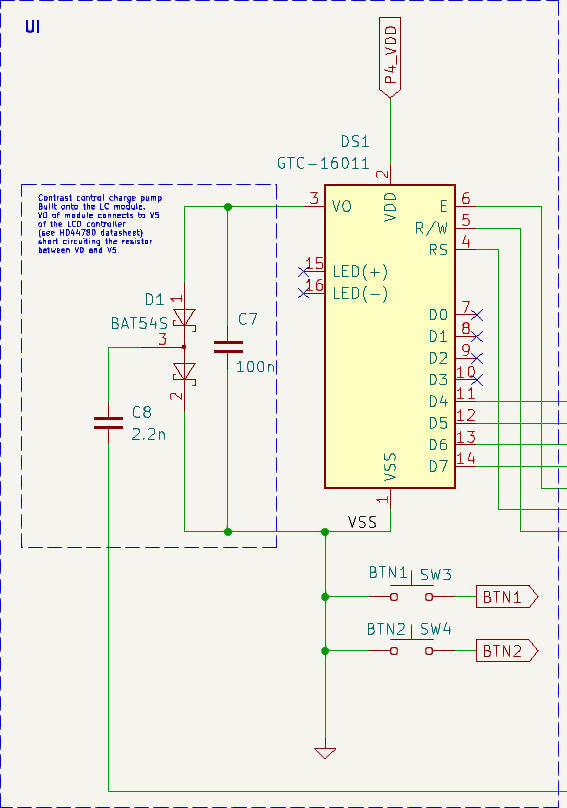
Display
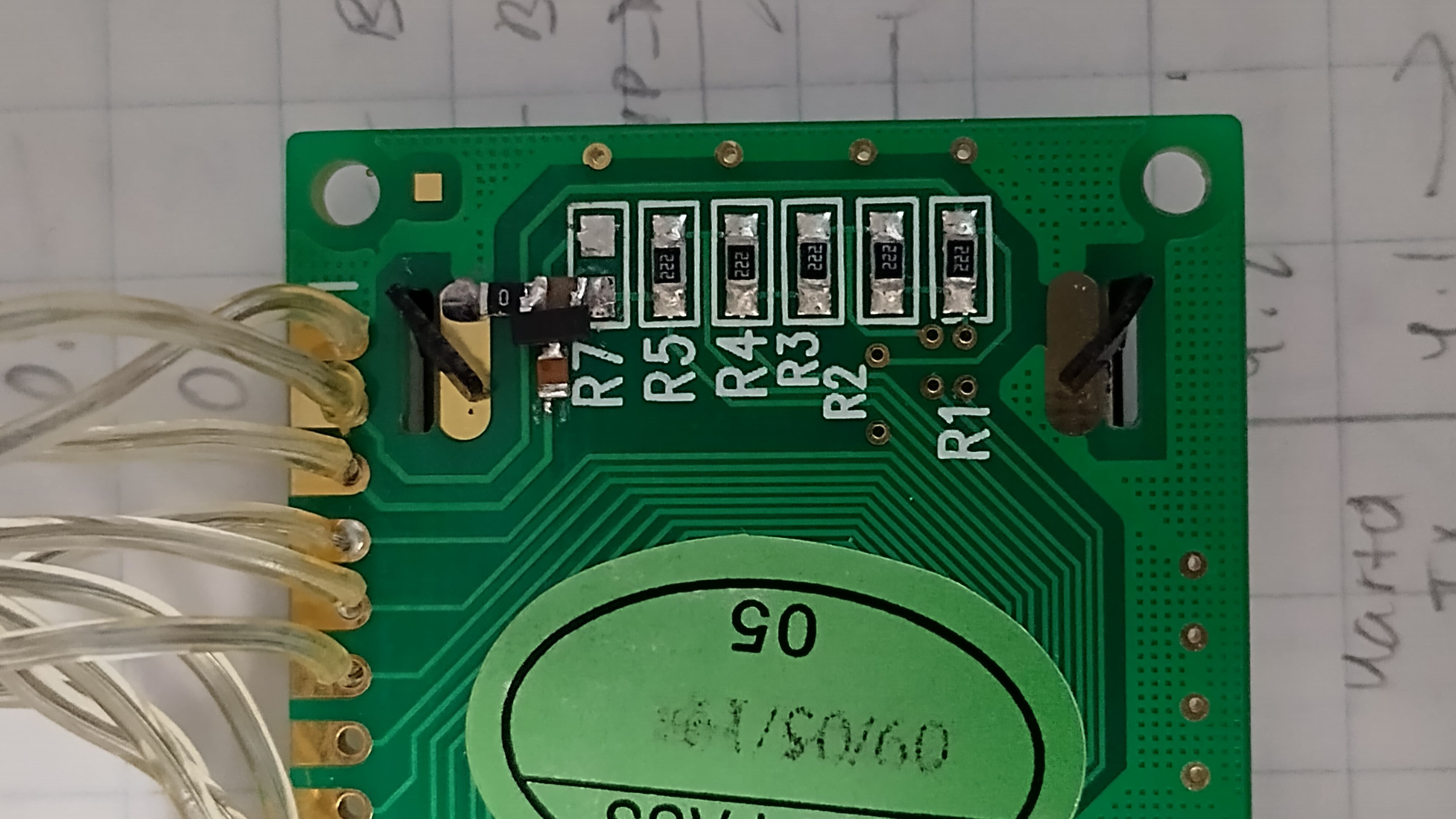
The display used in this project is a usual HD44780 type 16x1 display, GTC-16011. From a sell-off of a major distributor (0.85€ at that time, lifetime supply, again). All HW is running at 3.3 V but the display is a 5 V module. How to connect the display to a low voltage system? The ways are plenty, better and worse. My preferred choice is to take an advantage of the fact that the LCD controller is specified to work just fine with 3.3 V and only the glass requires 5 V. So the VDD of the module is set to 3.3V and GND to 0V. The glass voltage Vo is set to about -2 V using a simple charge pump. The charge pump is crafted to the module by replacing the lowest resistor of the glass voltage divider with it as shown below. The Vo pad of the module is used for the signal driving the charge pump which is generated by one PWM of the microcontroller. Only 2 capacitors and a BAT54S diode pair is needed.
An added bonus of the charge pump is that the contrast of the display can be adjusted electronically by changing the frequency of the PWM signal driving the Vo pin. Not implemented in this FW, though.
There are several views in the display. The following state diagram describes them and the navigation between them.
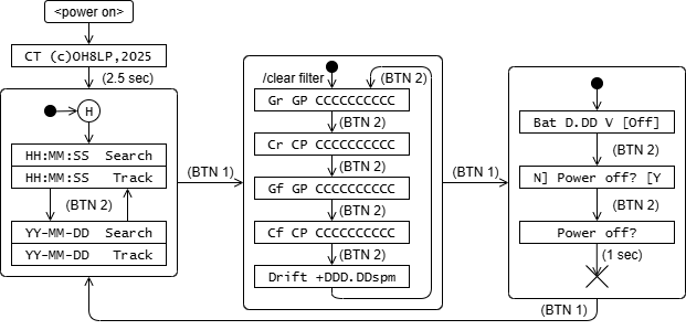
After power-on a brief copyright note is shown. Then the the display shows the time as reported by the GPS module.
Initially the time is incorrect as it comes from GPS that has not yet acquired any satellites. The status "Search" is shown eventually the time and date change to the correct UTC when satellites are found. When proper location fix is acquired the status changed from "Search" to "Track". Pressing the right button (BTN 2) switches between the time and date views.
The time/date view group remembers whether it was showing the time or the date when the other modes are visited with the left button (BTN 1), and shows the same when the view switches back to time/date group.
The next view group from the time/date, reached by pressing the left button, is the clock calibration group. It has five views.
The first four are GPS and clock sensor raw (Gr, Cr) and filtered (Gf, Cf) cycle counts. The comparison between the...
Read more »

 Ken Yap
 Mitsuru Yamada
 Vitalii